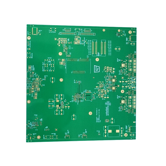
HDI PCB circuit board
Product description
HDI PCB circuit board is a kind of high-precision printed circuit. With the development of electronic technology, electronic products tend to be more and more high-density, light and thin, multi-functional, high reliability, small size and other characteristics, which forces the PCB board to need To develop in the direction of small size and thin thickness, and to meet the requirements of multi-function and high reliability of the product, HDI PCB circuit board was born. It has been widely used in aviation, automobile, medical, communication, Consumer products and other fields. HDI is the abbreviation of High Density Interconnector.
HDI PCB circuit boards are characterized by high reliability. In order to ensure the quality, when selecting materials, high-reliability materials should also be selected, especially boards. First, materials from brands such as Shengyi, Taiguang, and Taiyao should be selected. , Choose materials above minimum TG150 to prevent various quality problems caused by plates.
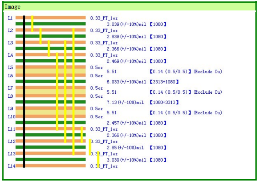
The stack structure of HDI PCB circuit boards is determined by the hole structure (determined by blind holes and buried holes). The structure of blind holes determines the order of HDI. The more times, the more the order of blind holes and the number of pressing, the more difficult it is to make, the longer the production process, and the longer the production cycle required.
In blind holes, stacked holes are designed. For example, the blind holes of L1-L2 and L2-L3 overlap. This is called stacked holes. The process difficulty is greater than that of non-stacked holes. more stringent control.
In HDI PCB circuit boards, in order to save wiring space, the conductive via hole is generally designed directly on the pad, and the size of the pad is small, which may easily lead to poor soldering or even failure to solder. In this case, it is necessary to The resin plug hole plus electroplating filling process is used to ensure the size of the pad to ensure good soldering performance. This design is a common design in HDI PCB circuit boards.

this is14layer3orderHDI PCBcircuit board(3 plus 8 plus 3)
Send Inquiry
