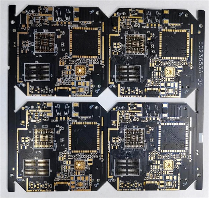
8L 2nd level HDI PCB circuit board
Product description
This product is 8 layers and 2 levelsHD PCBCircuit board, the hole structure in this data isL1-L2layer blind hole,L2-L3layer blind hole,L1-L3layer blind hole,L6-L7Blind hole,L7-L8Blind hole,L6-L8Blind hole,L3-L6buried via,L1-L8layer vias,L1-L3The layer blind holes will be decomposed intoL1-L2layer blind vias andL2-L3layer blind hole,L6-L8The layer blind holes will be decomposed intoL6-L7layer blind vias andL7-L8blind hole.According to the hole structure, the specific structure of the designed product is as follows:
| Press indication | 8-layer 2-level HDI PCB circuit board | Thickness(mm) |
| L1 | 0.33OZ electroplating to 1OZ | 0.035 |
| Media thickness | S1000HB PP1080H RC70 Percent | 0.072 |
| L2 | 0.33OZ electroplating to 1OZ | 0.035 |
| Media thickness | S1000HB PP1080H RC70 Percent | 0.066 |
| L3 | HOZ plating to 1OZ | 0.035 |
| Media thickness | S1000HB PP2116 RC56 Percent | 0.1 |
| L4 | 1OZ | 0.035 |
| substrate | CORE S1000H | 0.15 |
| L5 | 1OZ | 0.035 |
| Media thickness | S1000HB PP2116 RC56 Percent | 0.1 |
| L6 | HOZ plating to 1OZ | 0.035 |
| Media thickness | S1000HB PP1080H RC70 Percent | 0.66 |
| L7 | 0.33OZ electroplating to 1OZ | 0.035 |
| Media thickness | S1000HB PP1080H RC70 Percent | 0.072 |
| L8 | 0.33OZ electroplating to 1OZ | 0.035 |
Finished product thickness: 1.00 plus\/-0.1mm (including solder mask thickness)
The basic parameters of this product are as follows:
Number of layers: 8L (2nd level HDI PCB circuit board)
Material: Shengyi FR4 Tg150
Plate thickness: 1.0mm
Copper thickness:1\/1\/1\/1\/1\/1oz
Solder mask: matte black
Characters: white
Surface: Immersed gold 2uquot;, nickel thickness 3-6um
Minimum line width\/line spacing: 3\/3mil
Minimum BGA PAD: diameter 0.20mm
Has PTH half slot
Shipping size:112.83120.15mm\/4up
Send Inquiry
